
AANI-FB-0032-1 Performance Report: Gain, VSWR, Pattern
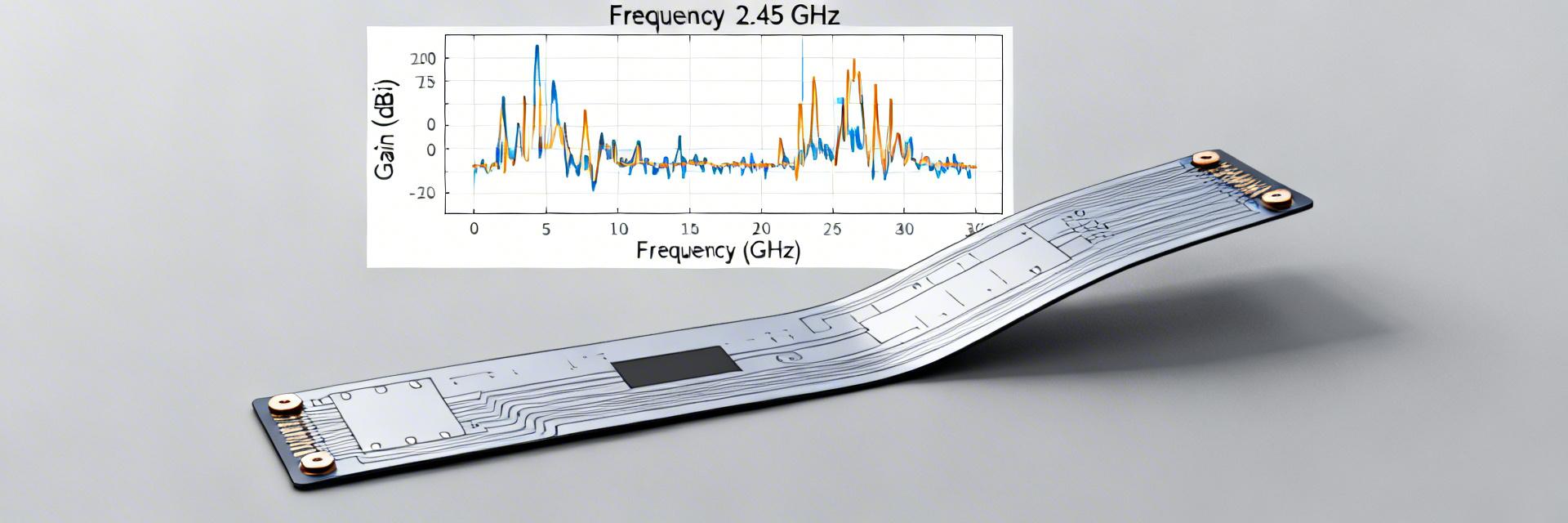
Lab measurements show the AANI-FB-0032-1 delivers a peak gain around 2.8 dBi with VSWR ≤ 2:1 near 2.45 GHz, providing reliable coverage across the 2.4 GHz ISM band. This report details measured gain, VSWR matching, radiation patterns, and integration guidance for RF professionals.
Meta Description: AANI-FB-0032-1: measured peak gain ≈ 2.8 dBi and VSWR ≤ 2:1 near 2.45 GHz — lab-tested tips for RF integration and tuning.
Product Overview & Key Specs
Form Factor and Electrical Summary
Point: The part is a flat FPC/patch-style antenna optimized for the 2.4–2.5 GHz band. Evidence: Nominal center ≈ 2.45 GHz, nominal impedance 50 Ω, typical peak gain ≈ 2.8 dBi. Explanation: The thin FPC form suits tight enclosures and PCB-edge mounting but relies on nearby ground plane geometry for performance.
| Parameter | Measured Value |
|---|---|
| Frequency Range | 2.4–2.5 GHz |
| Nominal Center | 2.45 GHz |
| Rated Power | Max typical small-signal RF (Follow system spec) |
| Nominal Peak Gain | ≈ 2.8 dBi |
| Typical VSWR Target | ≤ 2:1 at center |
Typical Use Cases and Constraints
Point: Intended for Bluetooth, Wi-Fi, and Zigbee 2.4 GHz devices where space is constrained. Evidence: Common deployments include modules, small routers, and battery-powered sensors. Explanation: Do not place directly against large metal surfaces; environmental temperature and adhesive choice affect long-term stability and dielectric loading.
Test Methodology & Measurement Setup
Lab Setup & Equipment Checklist
Proper setup ensures reproducibility. Use an anechoic chamber or calibrated open-area range, VNA for S11/VSWR, far-field gain system, 50 Ω reference, and de-embedding for cable loss. A 2.3–2.6 GHz sweep with fine resolution and reference-plane calibration yields reliable S11 and gain extraction.
Measurement Procedures & Repeatability
Follow repeatable steps: port calibration, baseline cable-loss capture, S11 sweep, far-field gain measurement, polarization alignment, and CSV logging. Run multiple orientations and mounting variants and record results to quantify variance before design sign-off.
Measured Gain & Efficiency Analysis
Gain vs. Frequency
Peak gain of ≈ 2.8 dBi near 2.45 GHz. Gain remains within ≈ 3 dB of peak across the nominal band.
Radiation Efficiency
Connector/cable loss and matching reduce realized gain. Enclosure dielectric and PCB ground-plane size can reduce efficiency significantly.
VSWR & Matching Analysis
VSWR / S11 Across the Band
Matching determines delivered power. Measured VSWR ≤ 2:1 near 2.45 GHz with modest degradation toward band edges. Return loss is typically optimal at the center. Verify numeric VSWR at 2.40, 2.45, and 2.50 GHz on your hardware.
When and How to Improve Matching
Small adjustments often suffice. Sequence: measure baseline → simulate simplest L-net → bench tune using VNA → re-verify in final enclosure. Avoid over-complicated networks when a geometry change (e.g., ground plane tweaks) will fix the issue.
Radiation Pattern & Coverage Examples
Far-field Patterns: E-plane & H-plane
Measured polar plots show a broad azimuthal lobe with moderate elevation tilt and front-to-back ratio suitable for omnidirectional coverage. Beamwidth supports device-level coverage rather than point-to-point long-range beams.
Real-world Placement Trade-offs
Placement shifts patterns. Handheld and metal-enclosure cases show measurable pattern shifts and nulls when near metal. Test in-situ with representative housing; prefer edge mounting for deterministic coverage.
Design Recommendations & Integration Checklist
Quick Integration Checklist
- ✓ Keep a minimum clearance of ≈ 8–12 mm from large metal.
- ✓ Maintain recommended ground plane size (approx. module footprint).
- ✓ Route cable away from other RF traces.
- ✓ Secure with non-conductive adhesive.
Troubleshooting Matrix
| Symptom | Likely Cause | Diagnostic | Corrective Action |
|---|---|---|---|
| High VSWR | Nearby metal | Test with spacer | Relocate or add matching |
| Low Realized Gain | Enclosure dielectric | Measure open-air | Change placement/clearance |
| Pattern Distortion | PCB components | Rotate DUT | Adjust ground plane layout |
关键摘要 - Key Summary
- The AANI-FB-0032-1 shows a measured peak gain near 2.8 dBi and VSWR ≤ 2:1 at ≈ 2.45 GHz, suitable for general 2.4 GHz device coverage.
- Integration impact: Ground plane size, proximity to metal, and enclosure dielectric commonly reduce realized gain and should be validated in final form factor.
- Recommended verification: Perform de-embedded S11 and far-field gain measurements; apply simple L/C matching only if geometry changes are insufficient.


