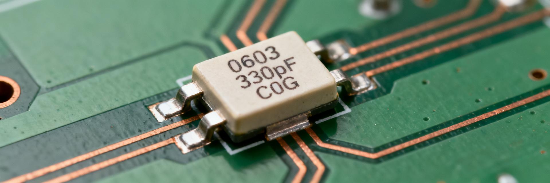
Designing with high-voltage ceramic capacitors often leads to confusion regarding specific package dimensions and electrical tolerances. This guide cuts through the noise, providing verified data for the GMT10CG271J50NT4 component. We will decode its exact pinout configuration, critical electrical specs, and integration best practices to ensure your circuit reliability from day one.
Component Overview and Package Identification
To effectively utilize the GMT10CG271J50NT4 in your designs, you must first understand its physical identity and naming conventions. Misidentifying the part number can lead to procurement errors or incorrect footprint layouts, which are costly to rectify during mass production.
Decoding the Part Number Structure
| Segment | Code | Meaning |
|---|---|---|
| Series | GMT | Manufacturer Series/Family Type |
| Size | 10 | Dimensional Size Class (Radial) |
| Dielectric | CG | Class I Ceramic (C0G/NP0) |
| Capacitance | 271 | 270 pF (27 x 10^1) |
| Tolerance | J | ±5% |
| Voltage | 50 | 50V DC Rated Voltage |
| Packaging | NT4 | Termination Style & Packaging Variant |
The alphanumeric code GMT10CG271J50NT4 contains precise engineering data. "CG" signifies the dielectric material, specifically Class I Ceramic (C0G/NP0), known for stability. "271" represents 270 pF, where the last digit is the multiplier. "J" indicates a ±5% capacitance tolerance. "50" denotes the rated voltage of 50V DC. Finally, "NT4" specifies the termination style, ensuring compatibility with standard through-hole assembly processes.
Physical Dimensions and Footprint Analysis
For PCB layout engineers, accurate mechanical drawings are paramount. The GMT10CG271J50NT4 features a radial leaded design. You should expect a body diameter approximately matching the "10" size designation, with lead spacing optimized for automated insertion machines. Verify the lead length against your board thickness to ensure proper solder joint formation. Unlike surface-mount devices, this through-hole component offers superior mechanical robustness, making it ideal for applications subject to vibration or thermal cycling. Always cross-reference the datasheet’s mechanical outline with your CAD library to prevent fitment issues.
Critical Electrical Specifications Deep-Dive
Beyond physical attributes, the electrical performance defines the GMT10CG271J50NT4's role in your circuit. Understanding these parameters ensures signal integrity and system longevity.
Capacitance Tolerance and Temperature Coefficient (C0G/NP0)
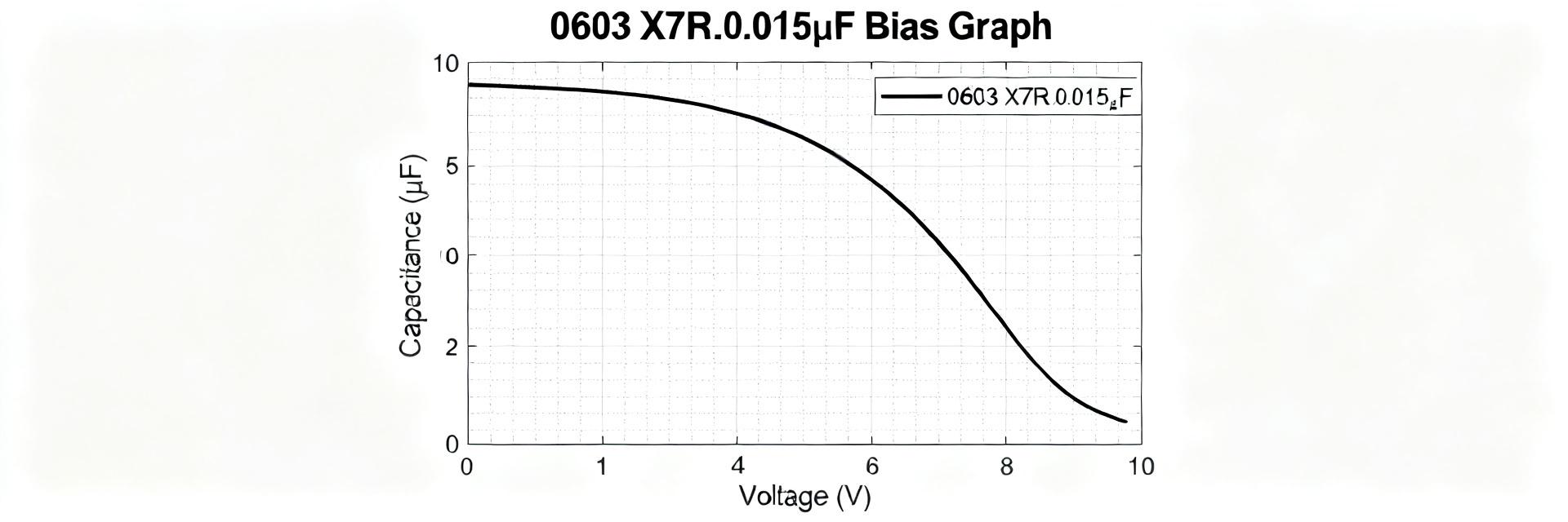
The C0G (or NP0) dielectric classification is the gold standard for precision. It exhibits a near-zero temperature coefficient, meaning capacitance remains stable across a wide operating range (-55°C to +125°C). With a "J" tolerance of ±5%, you can predict circuit behavior with high confidence. This stability is crucial for timing circuits, RF filters, and resonant networks where frequency drift due to temperature changes would degrade performance. In contrast to X7R or Y5V materials, C0G capacitors do not suffer from significant capacitance loss under bias voltage, maintaining their nominal value even when charged.
Rated Voltage and Leakage Current Limits
The 50V DC rating provides a safe margin for most low-to-mid voltage power rails. However, you must adhere to derating guidelines. While the absolute maximum rating is 50V, practical designs often operate at 80% of this limit to account for transient spikes. Leakage current for C0G ceramics is exceptionally low, typically measured in nanoamperes at room temperature. This characteristic makes the GMT10CG271J50NT4 suitable for coupling and decoupling applications where minimal DC offset error is required. High leakage could distort sensitive analog signals, so verifying spec sheets for worst-case leakage values at elevated temperatures is recommended.
Verified Pinout and Connection Diagrams
Correct connection is vital for functionality. Since this is a non-polarized ceramic capacitor, polarity concerns are minimal, but orientation affects parasitic inductance.
Terminal Configuration for Radial Leaded Variants
The GMT10CG271J50NT4 utilizes two terminals arranged radially. There is no positive or negative terminal; both leads are electrically equivalent. However, for high-frequency applications, the loop area formed by the leads and PCB traces creates parasitic inductance. You should orient the component such that the shortest possible trace path connects to the ground plane or adjacent components. Proper terminal alignment minimizes EMI emissions and improves signal fidelity in RF paths.
PCB Layout Guidelines for High-Frequency Stability
When placing the GMT10CG271J50NT4 on your PCB, keep leads as short as possible. Long leads increase ESL (Equivalent Series Inductance), raising the self-resonant frequency lower than desired. Use solid ground planes beneath the component to reduce impedance discontinuities. For bypass applications, place the capacitor close to the IC power pins. If multiple capacitors are used, arrange them to minimize mutual coupling effects. Following these layout rules ensures that the theoretical electrical specs translate into real-world performance.
Performance Characteristics in Practical Applications
Real-world behavior differs from ideal models. Analyzing frequency response and thermal dynamics helps you anticipate potential failure modes.
Frequency Response and Self-Resonant Frequency (SRF)
All capacitors have an SRF where they behave inductively rather than capacitively. For the GMT10CG271J50NT4 (270 pF), the SRF is typically in the hundreds of MHz range, depending on lead length. Above this frequency, impedance rises, reducing filtering effectiveness. You should calculate the expected operating frequency band of your circuit and ensure it falls well below the SRF. Using simulation tools to model the full impedance curve, including ESL and ESR (Equivalent Series Resistance), provides a clearer picture of attenuation characteristics across the spectrum.
Thermal Behavior Under Load Conditions
Ceramic capacitors generate heat primarily due to ripple current flowing through ESR. Although C0G has very low ESR, high-frequency switching applications can still induce thermal stress. Monitor the ambient temperature around the component. If the board operates in enclosed spaces, consider adding thermal vias near the pads to dissipate heat. Excessive temperature can accelerate aging, though C0G materials are highly resistant to degradation compared to Class II ceramics. Ensuring adequate airflow or conduction paths maintains long-term reliability.
Integration Best Practices and Safety Checks
Successful integration requires more than just selecting the right part. Manufacturing and handling protocols play a significant role.
Derating Strategies for Long-Term Reliability
Always apply voltage derating. A common rule of thumb is to operate at 50-60% of the rated voltage for high-reliability systems. For the GMT10CG271J50NT4, this means limiting continuous DC bias to 25-30V. This buffer protects against transients and extends lifespan. Additionally, derate based on temperature; if the ambient exceeds 85°C, further reduce the allowable voltage. Document these limits in your design review checklist to prevent accidental over-stressing during future revisions.
Common Pitfalls in Soldering and Handling
Through-hole components are susceptible to thermal shock during wave soldering. Preheat the board adequately to minimize stress on the ceramic body. Avoid mechanical stress on the leads after installation; bending leads excessively can crack the internal structure, leading to intermittent failures. When cleaning flux residues, use solvents compatible with epoxy coatings. Aggressive chemicals can damage the outer casing, exposing internal layers to moisture. Handle components with care to prevent chipping, which compromises dielectric strength.
Key Takeaways
- The GMT10CG271J50NT4 uses C0G dielectric for superior temperature stability and low losses.
- Part number decoding reveals 270pF capacitance, ±5% tolerance, and 50V rating.
- Minimize lead length in PCB layout to reduce ESL and maintain high-frequency performance.
- Apply voltage derating (50-60%) to ensure long-term reliability under dynamic loads.
- Avoid mechanical stress and thermal shock during soldering to prevent ceramic cracking.
Frequently Asked Questions
What does the "J" suffix mean in GMT10CG271J50NT4?
The "J" indicates a capacitance tolerance of ±5%. This tight tolerance is essential for precision circuits like oscillators or filters where exact frequency response is critical. Compared to looser tolerances like "K" (±10%), "J" ensures predictable manufacturing yields and consistent performance across batches.
Can I replace X7R capacitors with GMT10CG271J50NT4?
Yes, if the application demands high stability and low loss. X7R capacitors vary significantly with temperature and bias voltage. Replacing them with C0G types like the GMT10CG271J50NT4 improves accuracy in RF and timing circuits. However, verify that the physical size fits your existing footprint, as C0G parts may be larger for the same capacitance value.
How do I determine the Self-Resonant Frequency (SRF)?
SRF depends on capacitance and Equivalent Series Inductance (ESL). For the GMT10CG271J50NT4, consult the manufacturer’s frequency vs. impedance curves. Alternatively, measure it using a network analyzer. Shorter leads and closer placement to ground planes lower ESL, thereby increasing the SRF, allowing effective operation at higher frequencies.
Why is derating recommended for this capacitor?
Operating at 50-60% of the rated voltage (25-30V for this 50V part) protects against transient spikes and extends lifespan, especially in high-reliability systems. This strategy mitigates risks associated with voltage surges and thermal stress, ensuring the component operates within its optimal linear region.